Design Methodology
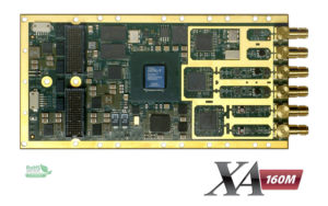
The XA XMC FPGA range are aimed at high rate applications with sample rates from a few MSPS to 615MSPS. The cards have upto 8 channels of Adc and/or Dac which are all directly connected to the FPGA. The FPGA also has 1024MB of DDR3 memory connected to it and x4 PCIe lanes to the host via the XMC connector. There is a sample clock generation onboard where necessary using a low phase noise PLL which can use an internal or external reference. The boards come complete with logic and example software to enable the boards to be used out of the box for data acquisition and/or waveform generation applications. Full support is provided locally by Entegra Solutions Ltd. We have completed many custom designs with these boards and are well placed to advise and provide custom solutions. The factory logic is fully documented and includes projects for development in Xilinx Vivado.
There are drivers available to use the XA boards in LabVIEW and Matlab. The driver is a DLL that configures the clock, trigger and streaming on the board. Adc samples are streamed via the onboard DDR3 memory to the host for processing in the chosen tool. Dac samples are generated on the host in the chosen tool and streamed via onboard DDR3 memory to the Dacs. When the board has both Adcs and Dacs, eg XA-160M, each direction has 512MB of virtual FIFO (vFIFO) in DDR3. When the board is either just Adcs or just Dacs, the direction has 1024MB of vFIFO. This is necessary to decouple the fast devices from the relatively slower processing of the host tool.

