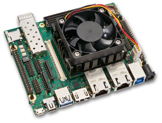
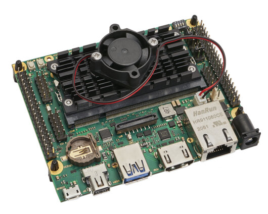
Enclustra Design-in Kits help shorten time-to-market for any Xilinx Zynq UltraScale+ MPSoC based application. Be it image processing, machine vision, test & measurement, communication or medical: With an Enclustra System-on-Module, the development time can be halved.
To shorten time-to-market as much as possible, Enclustra offers broad design-in support for their products and a comprehensive ecosystem, offering all required hardware, software and support materials. Detailed documentation and reference designs make it easy to get started. A user manual, user schematics, a 3D model, PCB footprints, differential I/O length tables and the Linux-based Board Support Package (BSP) are all provided. In combination with ready-made base boards and heatsinks, developing an FPGA project has never been easier.
AI/Machine Learning Examples Included
The design-in kits include 2 example applications, to get you started: AI face detection and image classification. They are based on ResNet50 and Xilinx Vitis AI. The ready made binaries as well as the sources are packed with the box – as well as the extensive documentation how to build it yourself.
What’s Inside the Box
- Enclustra Xilinx Zynq UltraScale+ MPSoC system-on-module/SOM
- Mars XU3 (MA-XU3-2CG-1E-D10) or
- Mercury XU5 (ME-XU5-4EV-1I-D11E)
- Base board
- Mars ST3 (MA-ST3-W) or
- Mercury+ ST1 (ME-ST1-W)
- USB camera
- Heatsink
- Fan
- Power supply
- USB cable
- MiniDP to DP cable
- Micro SD card
- Example applications:
- AI face detection
- Image classification
- Quick start guide
- User Manual
Available Resources
- Documentation
- Design support
- Design-in kit user guide
- User manuals
- Reference design
- PetaLinux board support package (BSP)
- Buildroot-based Linux BSP
- Module pin connection guidelines
- Master pinout
- Footprints
- 3D model
- IO net length
- User schematics
- Altium design files (base board)
- Application notes
Benefits
- A complete and powerful embedded processing system in the industry-standard SO-DIMM form factor
- Simple, low cost and yet rugged assembly
- Simple and low-cost integration due to the on-board standard interfaces (USB, Ethernet, CAN)
- Fast boot times and plenty of non-volatile memory space due to the NAND flash
- High-bandwidth program and data memory due to the high-performance hard-macro memory controller
- Lowest power consumption due to the high-efficiency DC/DC converters
Features
- Xilinx Zynq-7020 AP SoC in the CLG484 package (XC7Z020)
- ARM® dual-core Cortex™-A9
(32 bit, up to 766 MHz) - Xilinx Artix™-7 28nm FPGA fabric
- ARM® dual-core Cortex™-A9
- SO-DIMM form factor (67.6 x 30 mm, 200 pins)
- 108 user I/Os
- 12 ARM peripheral I/Os (SPI, SDIO, CAN, I2C, UART) shared with FPGA I/Os
- 96 FPGA I/Os (single-ended, differential or analog)
- Gigabit Ethernet and USB 2.0 OTG PHYs
- Up to 1 GB DDR3 SDRAM
- 512 MB NAND flash
- 64 MB quad SPI flash
- 3.3 V tolerant inputs
- Single 3.3 V supply voltage
Information on the product may change, please check the manufacturers website and page for the most up to date information, see the link at the top right of this page.


