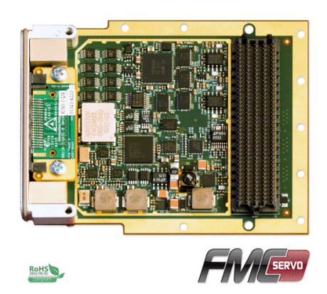
Features
- Eight A/D Input Channels
- 500 kSPS, 16-bit A/D
- Differential, Gain Programmable
- Eight D/A Output Channels
- 0.5µs Settling Time, 16-bit D/A
- ± 10V Output Range
- Sample clocks and timing and controls
- 10 MHz, ±250 ppb stability on- board reference
- Programmable PLL
- Programmable Clock Frequency as low as 3.05 kHz
- Integrated with FMC triggers
- FMC module, VITA 57.1
- High Pin Count no SERDES required
- Compatible with 2.5V VADJ
- Power monitor and controls
- 12 W typical
- Conduction Cooling per VITA 20 subset
- Environmental ratings for -40° to 85°C, 9g RMS sine, 0.1g2/Hz random vibration
Applications
- Industrial Instrumentation Systems
- Real-Time Control Systems
- Sensor Data Recording and Playback
- Machine Learning Systems
Overview
The FMC-SERVO module features eight simultaneously sampling A/D and DACs with an FPGA computing core. Low latency SAR A/D and fast-settling DACs support real-time servo control applications. The programmable input range and high input interface directly to many sensors, while the output is capable of driving many transducers. Front panel digital IO can be also be used as PWM or process controls.
Clock and trigger controls include support for consistent servo loop timing, counted frames, software triggering and external triggering. The sample rate clock is either an external clock or on-board programmable PLL clock source
The FMC-Servo power consumption is TBD W for typical operation. The module may be conduction cooled using VITA20 standard and a heat spreading plate. Ruggedization levels for wide-temperature operation from -40 to +85C operation and 0.1 g2/Hz vibration. Conformal coating is available.
Support logic in VHDL is provided for integration with FPGA carrier cards. Specific support for Innovative carrier cards includes integration with Framework Logic tools that support VHDL and Matlab developers. The Matlab BSP supports real-time hardware-in-the-loop development using the graphical block diagram Simulink environment with Xilinx System Generator for the FMC integrated with the FPGA carrier card.
Software tools for Innovative carrier cards include host development C++ libraries and drivers for Windows and Linux, 32/64-bit including RTOS variants. Application examples demonstrating the module features are provided.
* Sampling rates in an application depend on carrier and system design
Dataflow
The FMC modules come with logic to use them on the Innovative FMC hosts (ePC-K7, mini-K7 & others). The logic includes a sample streaming interface to the system processor. Please see the data flow diagram for the generic model.
The simplied data flow from Adc(s) to host application works as follows. Samples from the Adc(s) are clocked into the FPGA. The samples are packed where necessary for efficient use of the RAM chips. The RAM is used as a virtual FIFO to decouple the continuous stream of the Adc(s) from the block transfer nature of PCIe. The user application sets the packetsize. When a whole packet of data is available in the RAM, the PCIe DMA controller does a bus master transfer to the host memory. At configuration time the device drivers reserve physical memory for this purpose. When the transfer is complete, the DMA controller sends an interrupt to Malibu which then copies the packet from the busmaster area to virtual memory and then fires an event in the User application with a reference to the data.
The FMC host memory is usually 256MB or more. If the host can not consume the data as fast as the Adc(s) produces it, the memory fills with samples. This defines the longest continuous capture length possible.
The simplified data flow in the reverse direction for host to Dac(s) is similar. Onboard RAM is configured as a virtual FIFO between the PCIe and the Dac(s). When there is room in the RAM chips for a packet of samples, the PCIe DMA controller interrupts the host, which then signals the application to provide a packet of samples. The samples are copied from virtual memory to physical memory and then the PCIe DMA controller copies them into RAM. As data is flowed to the DAC(s) the RAM has more space for more packets and so the process is repeated.


