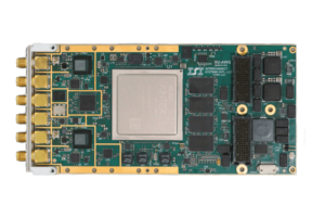
Features
- Two 16-bit, 12 Gsps, DAC channels:
- AD9162 DAC supports enhanced 2nd and 3rd Nyquist and “Frequency Doubling” 2x Modes
- Single-Ended AC-Coupled Outputs with Programmable DC Bias
- Digital Inverse Sinc Filter
- 48-Bit NCO
- Fixed Deterministic Latency
- Interpolation Filters: 1x (bypass mode), 2x, 3x, 4x, 6x, 8x,12x,16x, 24x
- Internal or External Reference Clock
- Internal TI LMK04828 or LMK04821 Master Reference PLL with Zero Delay Mode
- Individually Delay Controlled Reference Clock to Each DAC Slave PLL and FPGA
- Advanced Triggering Input Registered to JESD204B Reference Clock
- External Clock and Trigger Inputs
- Reference Clock Output
- XCKU060 Xilinx Kintex Ultrascale FPGA
- DDR4 DRAM in 2 banks each with 64 bit interface
- 4GB
- Up to 38.4GB/s total bandwidth (based on 100% data buss efficiency)
- QDR SRAM in 1 bank with 32 bit interface
- 4MB, 12x faster than DDR for random access applications (like FFTs)
Chipset
- Analogue to Digital Converter(s) = N/A
- FPGA = Xilinx Kintex Ultrascale XCKU060/085
- Digital to Analogue = AD9162
Applications
- Wireless Transmitter
- LTE, WiMAX Physical Layer
- RADAR, ECM, Electronic Warfare
- High Speed Playback
- IP development
Useful resources on Youtube
These videos may be helpful in learning about using the FPGA on this board.
Overview
The XU-AWG is an XMC module with two 8-lane high speed serial links: one on XMC connector P15, one on P16. These links can support several protocols (up to 8-lane PCIe on P15, Aurora, or user defined). The XU-AWG features two AC- coupled single-ended DAC outputs with programmable DC bias. The Analog Devices AD9162 high-speed/high performance DACs employ synchronization support, interpolation, fixed latency and unique output circuits supplying improved frequency synthesis in the 2nd and 3rd Nyquist zones.
A Xilinx Kintex Ultrascale XCKU060 FPGA with 4GB DDR4 RAM memory provides a high-performance DSP core for demanding applications such as RADAR and wireless IF generation. The close integration of the analog front-end, memory, and host interface with the FPGA enables real-time signal processing.
The XU XMC module couples a powerful multi-channel PCIe DMA architecture with a high performance 8-lane PCI Express link connected to the carrier. PCIe link speeds up to Gen3 are supported; however, the actual PCIe link performance depends on the XMC carrier as well as the host system.
The XU-AWG FPGA design can be fully customized using VHDL and the FrameWork Logic Devkit. Xilinx JESD204B IP license, purchased separately from Xilinx, is required for logic development.
A software development kit for host development includes C++ libraries and 64-bit drivers for Windows and Linux. An application demonstrating the module’s features, including streaming DAC samples from disk, is provided.
Dataflow
The board comes complete with working logic (Framework Logic) and software drivers (Malibu). Please see the data flow diagram.
The simplied data flow from Adc(s) to host application works as follows. Samples from the Adc(s) are clocked into the FPGA. The samples are packed where necessary for efficient use of the RAM chips. The RAM is used as a virtual FIFO to decouple the continuous stream of the Adc(s) from the block transfer nature of PCIe. The user application sets the packetsize. When a whole packet of data is available in the RAM, the PCIe DMA controller does a bus master transfer to the host memory. At configuration time the device drivers reserve physical memory for this purpose. When the transfer is complete, the DMA controller sends an interrupt to Malibu which then copies the packet from the busmaster area to virtual memory and then fires an event in the User application with a reference to the data.
The simplified data flow in the reverse direction for host to Dac(s) is similar. Onboard RAM is configured as a virtual FIFO between the PCIe and the Dac(s). When there is room in the RAM chips for a packet of samples, the PCIe DMA controller interrupts the host, which then signals the application to provide a packet of samples. The samples are copied from virtual memory to physical memory and then the PCIe DMA controller copies them into RAM. As data is flowed to the DAC(s) the RAM has more space for more packets and so the process is repeated.
On XU-TX the Dac memory is 4GB.
Support
The product comes with the following support items to help you with your project:
- Malibu Software, including
- Arb, Snap, Wave & Stream – example applications as sourcecode to setup the board for acquisition and waveform generation. Shows designer how to stream Adc samples to host file and stream from host to Dacs, written in C++.
- Drivers for Windows/Linux, 32 and 64 bit.
- Framework logic (source is extra cost)
- Makes the XU board act as a data acquisition card, using onboard DDR as huge virtual FIFO’s.
- iiForum
- Knowledgebase of previous users of the X6 board.
- Access to the XU engineers.
- Full hardware, software and firmware manuals as PDF.
- Telephone/email technical support from EnTegra DSP and Innovative Integration.


