Features
- Two independent 10GBASE-T interfaces with SR-IOV support
- 10 GbE/1 GbE/100 Mb/s copper PHYs integrated on-chip
- PCIe 2.1 (2.5GT/s or 5GT/s), Bus width — x1, x2, x4, x8
- Support for jumbo frames of up to 15.5 KB
- Flow control support: send/receive pause frames and receive FIFO thresholds
- TCP segmentation offload: up to 256 KB
- IPv6 support for IP/TCP and IP/UDP receive checksum offload
- Fragmented UDP checksum offload for packet reassembly
- Message Signaled Interrupts (MSI)
- Message Signaled Interrupts (MSI-X)
- Interrupt throttling control to limit maximum interrupt rate and improve CPU usage
- 128 transmit queues
- Receive packet split header
- Receive header replication
- Dynamic interrupt moderation
- DCA support
- TCP timer interrupts
- No snoop
- Relaxed ordering
(Note: module NIC requires enumeration and control via PCIe root master)
Chipset
Applications
- Remote embedded communications
- Wide area DAQ meshes
Overview
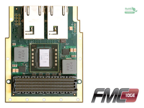
FMC-10GE provides two 10Gb Ethernet ports on a standard FMC module. Two, standard RJ45 connectors support connection to standard CAT6e networks providing high speed connectivity to PCs, servers embedded computers such as Innovative’s ePC products or custom, intelligent IO. Aggregated burst rates of up to 20 Gbps are achievable.
The two 10GE ports are fully independent on the module. Monitoring and control signals are mapped to the FMC interface for detection, loss- of-signal, rate and device control.
The FMC-10GE is fully electrically compatible with FMC (ANSI/VITA 57) specifications for IO module. Mechanically, the module will fit FMC sites, but the onboard, Intel X540 network controller (NIC) dissipates up to 13.5W necessitating use of a heat spreader attached to the carrier capable of managing the heat flow.
Unlike typical FMC modules, the NIC onboard the FMC-10GE must be enumerated and controlled as a PCIe device, typically under the control of a general purpose processor, rather than an FPGA. No VHDL-based control framework is available. Rather, this module must be used in conjunction with an FMC carrier capable of providing up to eight high- speed SERDES to the NIC which fully implement the PCIe 2.1 prototcol, such as FMC site 1 on Innovative’s ePC-K7 product.
The FMC-10GE works with legacy Gigabit Ethernet (GbE) switches and Cat 6A cabling. Install into an ePC-K7 and the auto-negotiation between 1 GbE and 10 GbE provides a smooth transition and easy migration to 10 GbE. When time and budget allows, 10GBASE-T switches can be added to your network to experience the full benefits of 10 GbE.
Software libraries and examples for C++ host development are provided. Application examples demonstrating the module features are provided for Innovative Integration platforms for Windows and Linux.
The combination of FMC-10GE and Innovative ePC-K7 provides a powerful, stand-alone, FPGA-based wireless transceiver.
Dataflow
The FMC modules come with logic to use them on the Innovative FMC hosts (ePC-K7, mini-K7 & others). The logic includes a sample streaming interface to the system processor. Please see the data flow diagram for the generic model.
The simplied data flow from Adc(s) to host application works as follows. Samples from the Adc(s) are clocked into the FPGA. The samples are packed where necessary for efficient use of the RAM chips. The RAM is used as a virtual FIFO to decouple the continuous stream of the Adc(s) from the block transfer nature of PCIe. The user application sets the packetsize. When a whole packet of data is available in the RAM, the PCIe DMA controller does a bus master transfer to the host memory. At configuration time the device drivers reserve physical memory for this purpose. When the transfer is complete, the DMA controller sends an interrupt to Malibu which then copies the packet from the busmaster area to virtual memory and then fires an event in the User application with a reference to the data.
The FMC host memory is usually 256MB or more. If the host can not consume the data as fast as the Adc(s) produces it, the memory fills with samples. This defines the longest continuous capture length possible.
The simplified data flow in the reverse direction for host to Dac(s) is similar. Onboard RAM is configured as a virtual FIFO between the PCIe and the Dac(s). When there is room in the RAM chips for a packet of samples, the PCIe DMA controller interrupts the host, which then signals the application to provide a packet of samples. The samples are copied from virtual memory to physical memory and then the PCIe DMA controller copies them into RAM. As data is flowed to the DAC(s) the RAM has more space for more packets and so the process is repeated.


